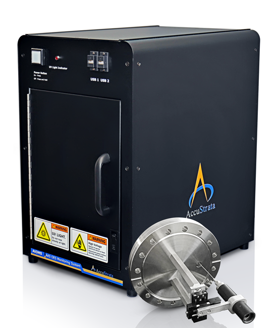
AtOMS Atomic Spectroscopy System
AccuStrata’s Atomic Optical Monitoring System (AtOMS) is a combined atomic absorption and optical emission spectrometry platform, which uses a variety of fiber-optics sensors installed on the customer’s equipment, real-time absorption/emission data analysis of and in situ parameter characterization combined with process modeling, deep learning, and predictive process control.
How Atomic Absorption Spectroscopy (AAS) and Physical Vapor Deposition (PVD) works
Scroll down to the bottom of the page to see more explanation videos.
Unique
What sets AtOMS apart is our novel approach to process control. By integrating Atomic Absorption and Optical Emission Spectroscopy (AAS & OES) with our specially engineered components, this patented system offers you capability beyond what is currently available elsewhere. The fiber optic sensor approach allows installation of a variety of custom settings without retrofitting of the customer’s equipment.
Customizable
A single system can monitor up to 4 chemical elements simultaneously, displaying each individual element deposition rate and the composition of the compound film as it is deposited/etched. With over 60 elements available, we can target the unique materials you require. In addition, up to three probe channels enable monitoring support distributed monitoring for multi-step, multi-chamber processes or more detailed data acquisition on process uniformity in a single chamber.
Adaptive
AtOMS is designed to accommodate your existing chamber configurations and geometries. Installation versatility is facilitated by our flexible fiber optic sensors specially designed by our engineers for optimal performance for the most demanding optical emission and atomic absorption spectrometry applications.
The Customer
Thin Film Processes:
Physical Plasma Etching
Physical Vapor Deposition (PVD)
Monitoring For:
Developing & scaling up new processes
Optimizing & stabilizing existing processes
Transferring processes to new systems
Increasing manufacturing yield / throughput
Specifications
System Module
- The main box houses the metrology platform as well as a full PC system.
- HDMI video output
- 2x USB connections for the PC
- On board Windows 10 platform
- AtOMS Control software (provided upon request)
- Single system supports up to 3 probe beam outputs, allowing:
- Installation into 3 separate chambers or chamber compartments
- Installation of 3 probe beams in a single chamber for uniform monitoring of very large, oddly shaped, or irregularly moving substrates
- PC Display, keyboard, mouse (provided)
- Power Requirements
- 120 V, 3 A
- Element specific Hollow cathode lamp(s) (HCL)
- up to 2 HCL can monitor up to 4 chemical elements at the same times
- act as a light source to probe the plasma
- HCL wavelength is specific to the monitored element/s
- Single system supports up to 2 HCL per system, with lamps that can emit 1, 2, or 3 elements simultaneously.

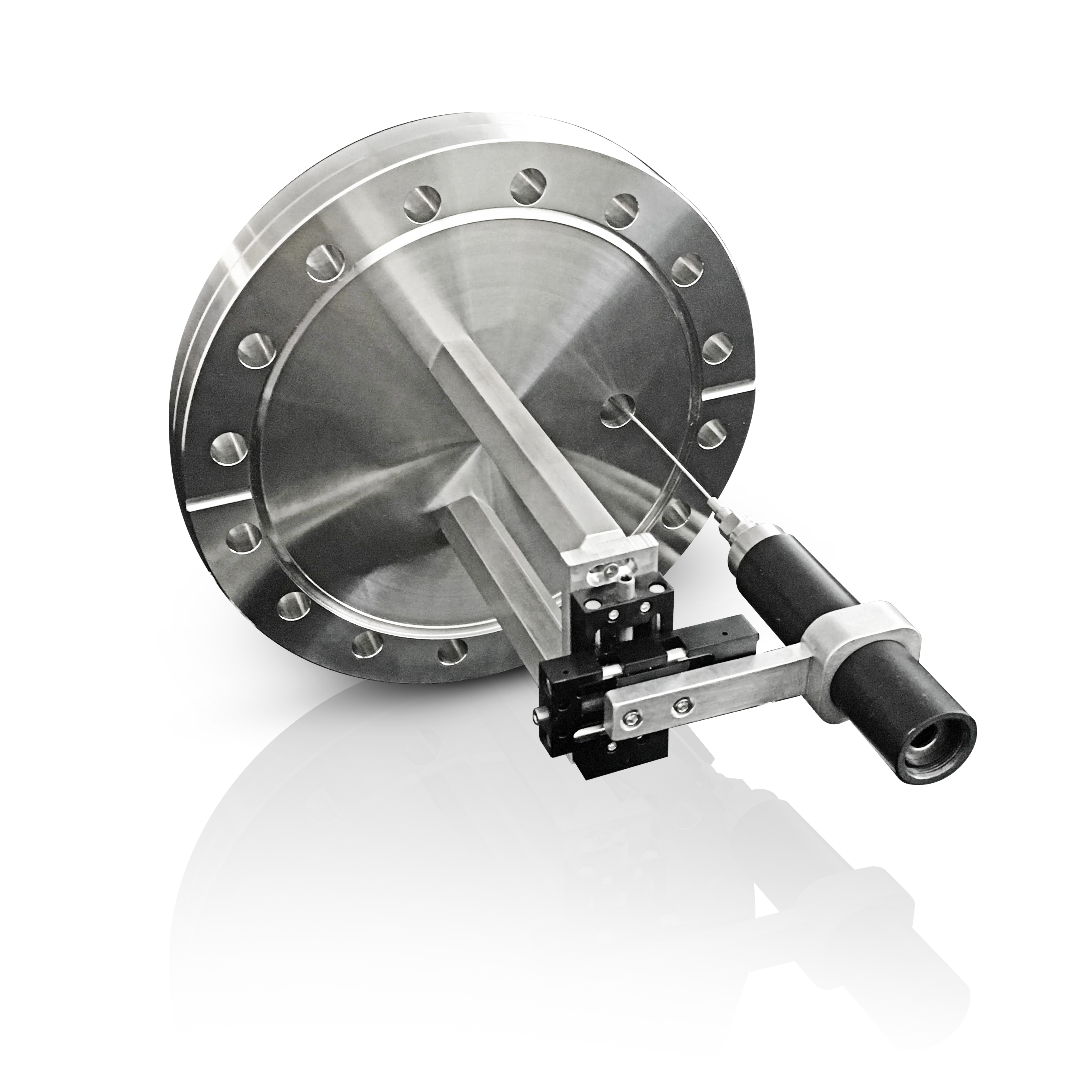
Optical Sensors
- Portable deep UV fiber optics optical collimators
- Connected to the hardware by flexible fiber optics cables that extend from the back of the main box.
- Installable externally through quartz viewports (supplied by AccuStrata) or internally in the chamber using metal-coated fibers for unprecedented monitoring accuracy
- Protected against coating deposition using AccuStrata’s proprietary means for prolonged deployment on the customer’s equipment
Consumables
- Hollow Cathode Lamp (HCL lifetime is ~1,000 working hours)
- Inexpensive quartz slides for protection of customer’s chamber viewport (when needed)


AtOMS Capabilities
- Deposition rates of multiple elements simultaneously
- Etching of very small areas on large wafers
- Concentration of elements during multi-element depositions
- Chemical composition of compound films and alloys
- Monitors optically opaque materials, metals and alloys
- >60 individual chemical elements can be monitored
- Multiple chambers or chamber compartments monitored simultaneously
- 3-beam distributed monitoring over the wafer for uniformity control
- Agnostic to substrate shape, position and motion
- Control of extremely thin films (<3 nm)
- Control of very high deposition/etching rates
- Deposition/etching rate accuracy – element specific (typical momentary rate ±0.01Å/s)
- Film composition accuracy ±0.05 atomic % (element specific)
Competition
| Capability | Atoms | Optical Monitoring | Crystal Monitor |
|---|---|---|---|
| Simultaneous multi-element deposition rate monitoring | ✓ | x | x |
| Monitoring with multiple probe beams/sensors from a single system | ✓ | ✓ | x |
| Monitoring multiple vacuum chambers or compartments with a single system. | ✓ | x | x |
| Monitoring element concentration of multi-element depositions | ✓ | x | x |
| Monitoring of multi-element chemical composition | ✓ | x | x |
| >60 different chemical elements can be uniquely monitored | ✓ | x | x |
| Monitoring extremely thin films (<3nm) | ✓ | x | x |
| Controlling very high deposition rates | ✓ | x | ✓ |
| Deposition rate accuracy of 0.01 Å/sec | ✓ | ✓ | x |
| Film composition accurace better than 0.1 atomic % | ✓ | x | x |
| Monitoring optically opaque materials, metals and alloys | ✓ | x | ✓ |
AccuStrata AtOMS Technology Explained
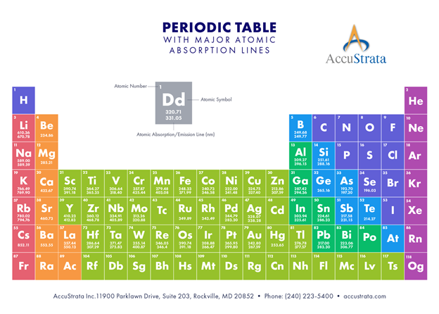
Periodic Table
How Atomic Absorption Spectroscopy works
Thin film deposition by Physical Vapor Deposition or PVD is a proven technique for a diverse range of applications including multi-layer x-ray optics, coatings of aerospace, automotive and machine tool components, depositing solar materials or thin films in electronic, semiconductor and medical device production. The AtOMS (Atomic Optical Monitoring System) from Accustrata uses Atomic Absorption Spectroscopy or AAS and Optical Emission Spectroscopy (OES) to address the need for in-situ, real time monitoring of the deposition process to ensure film quality and yield.
In PVD, metals, alloys, compound semiconductors or other materials are vaporized, resulting in a cloud of atoms, which are precisely deposited onto a substrate to create a thin film. The layer can be as thin as a few Angstroms. AAS is a real time optical metrology technique to monitor this process as it happens.
To achieve this unique capability, a probe beam of light at a wavelength, specific to the element it needs to monitor is passed through the plasma. Specific hollow cathode light sources are used that uniquely match the wavelength to the element under study. The vaporized atoms absorb the probe light proportionally to their atomic concentration. By monitoring this absorption, Atoms provides a unique method of process monitoring. Software is used to calculate the atomic concentration of the individual elements of interest and correlates the film deposition rate, thickness and chemical composition.
HCL light sources can be selected to monitor over 60 elements and some HCLs can emit lines to monitor 2 elements, and with two such lamps 4 elements can be measured simultaneously. This provides for monitoring the chemical composition of the growing film in real time. In addition, the unique, fiber optic-based approach supports multi-sensor capabilities for mapping of the entire area of the substrate to control uniformity.
In many applications, Atomic Spectroscopy has proven to be the best choice compared to more traditional monitoring techniques. It can be applied to non-transparent films such as metals and alloys, extremely thin films and complex multi-layers, as well as films deposited on curved or moving substrates.
